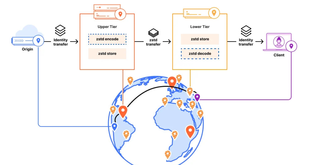
Cloudflare recently described a prototype called Cache Transcoding that compresses eligible cache content, mainly uncompressed text such as HTML, JSON, CSS, and JavaScript, using Zstandard before storing it on disk. The hyperscaler estimates that the approach could provide petabytes of additional effective cache capacity, although broader testing is still needed. By Renato Losio
Cloudflare recently described a prototype called Cache Transcoding that compresses eligible cache content, mainly uncompressed text such as HTML, JSON, CSS, and JavaScript, using Zstandard before storing it on disk. The hyperscaler estimates that the approach could provide petabytes of additional effective cache capacity, although broader testing is still needed.
Plug a phone into a modern charger and the first 10 minutes are impressive. The next 20 are not.
This is not a defect. It’s the connected device protecting itself. As temperature rises during charging, a smartphone’s battery management system reduces the current it will accept, because heat accelerates the chemical degradation that permanently reduces battery capacity. The charger may be capable of delivering more, but the device simply stops taking it.
For anyone building products in the
Plug a phone into a modern charger and the first 10 minutes are impressive. The next 20 are not.
This is not a defect. It’s the connected device protecting itself. As temperature rises during charging, a smartphone’s battery management system reduces the current it will accept, because heat accelerates the chemical degradation that permanently reduces battery capacity. The charger may be capable of delivering more, but the device simply stops taking it.
For anyone building products in the portable power category, this creates an uncomfortable gap between specification and experience. A device rated at 25 watts is accurate in the sense that it can deliver 25 watts. Whether it delivers 25 watts for the duration of a charge is a different question, and one the specification does not answer.
The specification gap
The gap matters commercially because it is invisible at the point of purchase and obvious in use.
Consumers compare wattage figures on packaging. They don’t compare thermal curves, because thermal curves are not published publicly. The result is a category where products differentiate on a number that describes peak output rather than sustained output, and where the actual user experience of two products with identical specifications can diverge substantially.
This is particularly acute in magnetic wireless charging. Inductive power transfer generates heat at both the transmitting and receiving coils, and the magnetic attachment that makes these products convenient also places the heat source in direct contact with the device it is charging. Convenience and thermal performance are working against each other by design.
The industry’s response for the past several years has been materials science. Graphite sheets, thermal interface materials, conductive housings, and heat-spreading layers have all improved how efficiently accumulated heat moves away from the source. Each generation has been incrementally better than the last.
But passive dissipation has a structural limitation: it can only move heat that has already been generated, and only as fast as the surrounding air will accept it. In a sealed, pocket-sized enclosure, that ceiling arrives quickly. Improving the materials slows the rate of temperature rise. It does not prevent the temperature rise.
Moving from dissipation to removal
The alternative is active thermal management, which is standard in stationary electronics and largely absent from portable ones for reasons that are easy to understand. Fans add volume, weight, moving parts, and noise. In a product category defined by portability, each of those is a meaningful cost.
At Anker, which manufactures charging and power products, engineering teams spent the past several development cycles working on whether that tradeoff could be made acceptable rather than eliminated. The approach involves several interacting systems: a micro centrifugal fan, dual airflow channels routed to avoid interference with the magnetic array, a three-layer graphene heat-spreading layer, and a control algorithm that modulates fan speed based on real-time temperature and battery state rather than running at a fixed rate. The result is that the Anker MagGo Power Bank 2 Pro has become the world’s fastest and coolest wireless power bank.
In internal testing, at 77 °F (25 °C) ambient, the back of the power bank stays below 96.8 °F (36 °C) throughout wireless charging, 21.6 °F (12 °C) below the international standard limit of 118.4 °F (48 °C), for a comfortable grip. Comparable magnetic power banks in the same testing typically reached 113 °F (45 °C) or higher within 20 minutes. The functional consequence is that the connected device does not reach the threshold at which it begins reducing charge acceptance, so 25 watts of Qi2.2 magnetic wireless charging is delivered as a working rate rather than an opening rate. In practice, an iPhone 17 Pro reaches 50% charge in 25 minutes. The Anker MagGo Power Bank 2 Pro’s premium performance in both charging speed and thermal management is certified by SGS, an independent testing and certification company.
The same principle applies in reverse. Recharging a power bank generates heat too, which is why devices in this category are often slow to recharge, leaving users with an empty accessory at the moment they need it. Active cooling during input allows the unit to accept 45 watts and reach 80% in 52 minutes.
What this suggests about the category
There is a broader pattern here worth naming, because it is not unique to charging.
When a category improves along a single axis for long enough, the constraint usually migrates somewhere else. Charging spent a decade optimizing power delivery. Power delivery is now, for most practical purposes, solved: the electronics can supply more energy than the receiving device is willing to accept. The binding constraint moved to thermal management, and the industry continued optimizing the axis it had always optimized, because that is the axis the specifications describe.
Recognizing when a constraint has moved is difficult precisely because the old metric keeps improving. Wattage figures have continued to climb. Products have continued to get faster on paper. The measurement stayed valid while quietly ceasing to describe the thing users experience.
For product organizations, the practical question is whether their specifications still measure the constraint or merely measure the capability. The two align until the constraint shifts and specifications rarely shift with it.
The transparency problem
A second implication follows from the first. If sustained performance differs meaningfully from peak performance, and if only peak performance is disclosed, then buyers cannot evaluate the products in front of them.
This is one reason Anker is adding displays on charging products. The Anker MagGo Power Bank 2 Pro shows real-time power, temperature, battery level, and estimated time remaining. Some of that is user convenience. But some of it is a Anker stating a deliberate position—this category deserves to have the complete and accurate data made transparent to all.
Anker expects independent reviewers to test these claims and considers our internal numbers to be the correct outcome. The gap between specification and experience closes faster when the experience is measurable. The Anker MagGo Power Bank 2 Pro will be available in the U.S. on September 17, 2026.
This content was produced by Anker. It was not written by MIT Technology Review’s editorial staff.
Throughout the history of the computer chip, engineers have treated waste heat as an inevitable cost of a calculation. Hannah Earley, however, thinks it’s a design choice. Earley, 31, is cofounder and chief technology officer of Vaire Computing, a startup building chips that recycle energy usually thrown away as heat—a strategy known as reversible computing. Ultimately, she thinks, this approach could help make data centers (and our laptops and phones) much more energy efficient.
When conven
Throughout the history of the computer chip, engineers have treated waste heat as an inevitable cost of a calculation. Hannah Earley, however, thinks it’s a design choice. Earley, 31, is cofounder and chief technology officer of Vaire Computing, a startup building chips that recycle energy usually thrown away as heat—a strategy known as reversible computing. Ultimately, she thinks, this approach could help make data centers (and our laptops and phones) much more energy efficient.
When conventional computer chips perform calculations, they erase the information they no longer need along the way, dissipating energy as heat in the process. Earley compares the approach to racing through a city only to pump the brakes at every intersection: The car loses momentum and must burn more fuel to accelerate again. Reversible computing aims to keep the momentum going—instead of erasing information from the intermediate steps in a calculation, the circuit retains it, making it possible to run the computation backward and recover some of the energy.
While the idea was first proposed more than 50 years ago, it proved impractical to implement with existing transistors and circuits. Earley, though, has completely rethought the hardware needed to make energy recovery work. She designed a patent-pending type of resonator—a microscopic chip component that stores recovered energy for later reuse. “It’s really a glorified pendulum,” she says. Last year, Vaire announced a key breakthrough: a chip with a resonator that recovered more energy than it lost, even after the energy needed to power the component was taken into account. For a subfield that has existed mostly in theory, the result was proof of life.
“It’s clear they have something interesting,” says Igor Markov, a researcher in electronic design automation and a former professor at the University of Michigan, Ann Arbor. Still, he says, the technology is quite early stage; the company will need “a series of increasingly realistic and convincing demonstrations to attract the industry support needed for commercialization.”
She gradually became convinced that the connection between information, energy, and heat could change computers forever.
Earley’s journey into chip design started sooner than most. She began programming around the age of nine, starting with high-level coding for the web before digging into other programming languages like Perl and Java. She continued progressing to more and more abstract layers of computing, until she got all the way down to transistors.
She eventually enrolled in a PhD program at the University of Cambridge under the computational biologist Gos Micklem. She started out studying how materials such as DNA could be used to perform calculations, but a few months in, Micklem sent her the 1999 PhD thesis of Michael Frank, a pioneer in reversible computing. Earley read it once, felt skeptical, read it again, and sat with it for a few weeks. She gradually became convinced that the connection between information, energy, and heat could change computers forever.
The fascination completely redirected her PhD work. Earley studied the physical limits of computation and built software that could turn ordinary programs into reversible ones. “Eventually I wouldn’t let her put my name on any of her papers, because I felt that I couldn’t really stand up and give a proper talk about them,” Micklem recalls. “It was her stuff.”
After completing her degree in 2021, Earley met Rodolfo Rosini, a technology entrepreneur and investor. The pair cofounded Vaire that same year, and the company has since raised more than $12 million, hired Frank as a senior scientist, and begun turning the vision of reversible computing into real hardware.
Innovation, however, doesn’t happen overnight. During the winter of 2022 in Grinnell, Iowa, Earley spent weeks in her now-wife’s basement apartment as the wind chill outside reached roughly −40 °F, covering a whiteboard over and over again with schematics for the core piece of circuitry needed to make reversible logic work. By the time the design finally came together, after the couple had escaped the cold for Las Vegas, it felt less like an aha moment and more like a gradual wave of relief. “I’m not completely out of my depth,” she remembers feeling.
Earley and her colleagues’ next challenge is making their drastically different chip fit into familiar devices and manufacturing systems. She believes that’s where the future lies—not in further refining existing chips but in rebuilding them from the ground up with an eye toward reversibility. “I want to tackle every part of how computers are built,” Earley says, “and rethink it in these terms.”
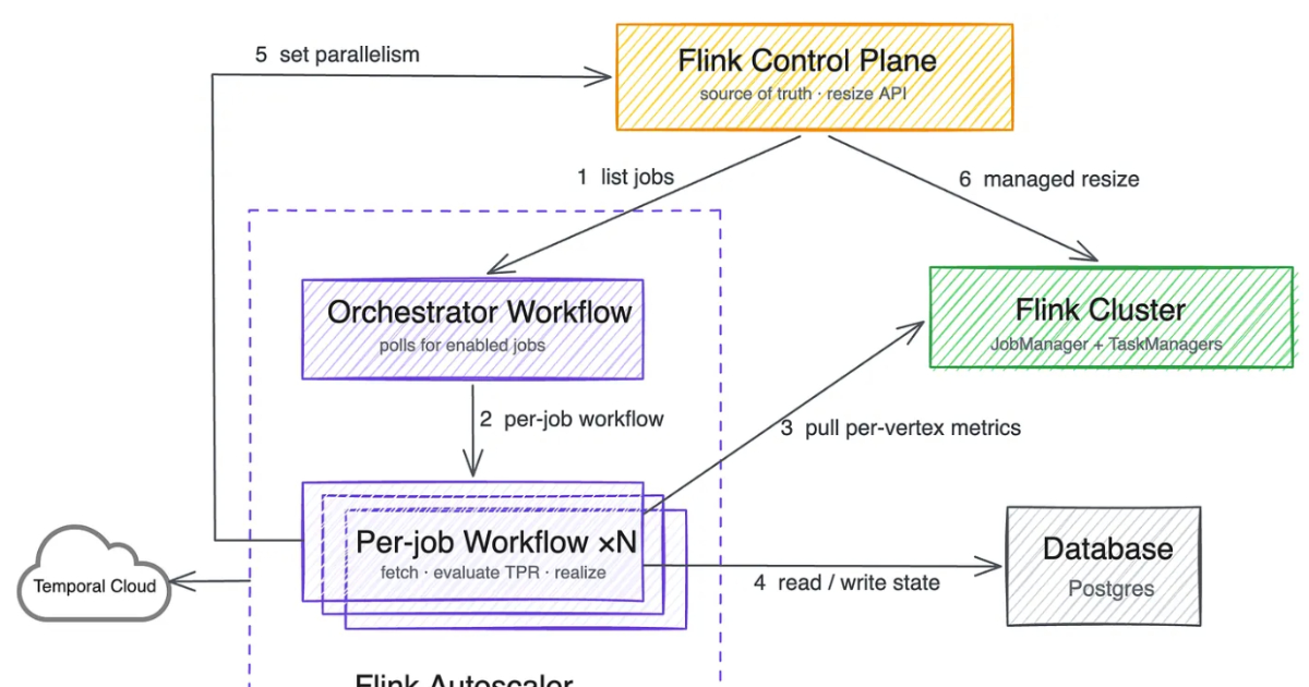
Netflix is moving toward the open-source Apache Flink Autoscaler for more than 30,000 streaming jobs across multiple AWS regions. The operator-level approach addresses limitations of Netflix’s cluster level autoscaler for complex, stateful pipelines. Netflix reports a 58% reduction in annualized Flink compute expenditure for one team, saving approximately $1.1 million annually. By Leela Kumili
Netflix is moving toward the open-source Apache Flink Autoscaler for more than 30,000 streaming jobs across multiple AWS regions. The operator-level approach addresses limitations of Netflix’s cluster level autoscaler for complex, stateful pipelines. Netflix reports a 58% reduction in annualized Flink compute expenditure for one team, saving approximately $1.1 million annually.
Gemma 4 can be paired with multi-token prediction (MTP) drafters that use speculative decoding to generate multiple tokens in parallel, allowing the model to verify them in a single pass and achieve up to ~3× faster inference without quality loss. By Sergio De Simone
Gemma 4 can be paired with multi-token prediction (MTP) drafters that use speculative decoding to generate multiple tokens in parallel, allowing the model to verify them in a single pass and achieve up to ~3× faster inference without quality loss.
Human-made glass is thousands of years old. But it’s now poised to find its way into the AI chips used in the world’s newest and largest data centers.
This year, a South Korean company called Absolics is planning to start commercial production of special glass panels designed to make next-generation computing hardware more powerful and energy efficient. Other companies, including Intel, are also pushing forward in this area.
If all goes well, such glass technology could reduce the energy
Human-made glass is thousands of years old. But it’s now poised to find its way into the AI chips used in the world’s newest and largest data centers.
This year, a South Korean company called Absolics is planning to start commercial production of special glass panels designed to make next-generation computing hardware more powerful and energy efficient. Other companies, including Intel, are also pushing forward in this area.
If all goes well, such glass technology could reduce the energy demands of the sorts of high-performance computing chips used in AI data centers—and it could eventually do the same for consumer laptops and mobile devices if production costs fall.
The idea is to use glass as the substrate, or layer, on which multiple silicon chips are connected. This form of “packaging” is an increasingly popular way to build computing hardware, because it lets engineers combine specialized chips designed for specific functions into a single system. But it presents challenges, including the fact that hardworking chips can run so hot they physically warp the substrate they’re built on. This can lead to misaligned components and may reduce how efficiently the chips can be cooled, leading to damage or premature failure.
“As AI workloads surge and package sizes expand, the industry is confronting very real mechanical constraints that impact the trajectory of high-performance computing,” says Deepak Kulkarni, a senior fellow at the chip design company Advanced Micro Devices (AMD). “One of the most fundamental is warpage.”
That’s where glass comes in. It can handle the added heat better than existing substrates, and it will let engineers keep shrinking chip packages—which will make them faster and more energy efficient. It “unlocks the ability to keep scaling package footprints without hitting a mechanical wall,” says Kulkarni.
Momentum is building behind the shift. Absolics has finished building a factory in the US that is dedicated to producing glass substrates for advanced chips and expects to begin commercial manufacturing this year. The US semiconductor manufacturer Intel is working toward incorporating glass in its next-generation chip packages, and its research has spurred other companies in the chip packaging supply chain to invest in it as well. South Korean and Chinese companies are among the early adopters. “Historically, this is not the first attempt to adopt glass in semiconductor packaging,” says Bilal Hachemi, senior technology and market analyst at the market research firm Yole Group. “But this time, the ecosystem is more solid and wider; the need for glass-based [technology] is sharper.”
Fragile but mighty
Chip packaging has relied on organic substrates such as fiberglass-reinforced epoxy since the 1990s, says Rahul Manepalli, vice president of advanced packaging at Intel. But electrochemical complications limit how closely designers can place drilled holes to create copper-coated signal and power connections between the chips and the rest of the system. Chip designers must also account for the unpredictable shrinkage and distortion that organic substrates undergo as chips heat up and cool down. “We realized about a decade ago that we are going to have some limitations with organic substrates,” says Manepalli.
These glass substrate test units were photographed at an Intel facility in Chandler, Arizona, in 2023.
INTEL CORPORATION
Glass may help overcome a lot of these limitations. Its thermal stability could allow engineers to create 10 times more connections per millimeter than organic substrates, says Manepalli. With denser connections, Intel’s designers can then stuff 50% more silicon chips into the same package area, improving computational capability. The denser connections also enable more efficient routing for the copper wires that deliver power to the chip. And the fact that glass dissipates heat more efficiently allows for chip designs that reduce overall power consumption.
“The benefits of glass core substrates are undeniable,” says Manepalli. “It’s clear that the benefits will drive the industry to make this happen sooner rather than later, and we want to be one of the first ones who do it.”
However, working with glass creates its own challenges. For one thing, it’s fragile. Glass substrates for data center chip packages are made from panels that are only about 700 micrometers to 1.4 millimeters thick, which leaves them susceptible to cracking or even shattering, says Manepalli. Researchers at Intel and other organizations have spent years figuring out how to use other materials and special tools to integrate the glass panels safely into semiconductor manufacturing processes.
Now, Manepalli says, Intel’s research and development teams are reliably fabricating glass panels and churning out test chip packages that incorporate glass—and in early 2025 they demonstrated that a functional device with a glass core substrate could boot up the Windows operating system. It’s a significant improvement from the early testing days, when hundreds of glass panels got cracked every couple of days, he says.
Semiconductor manufacturers already use glass for more limited purposes, such as temporary support structures for silicon wafers. But the independent market research firm IDTechEx estimates there’s a big market for glass substrates, one that could boost the semiconductor market for glass from $1 billion in 2025 to as much as $4.4 billion by 2036.
The material could have additional benefits if it takes off. Glass can be made astoundingly smooth—5,000 times smoother than organic substrates. This would eliminate defects that can arise as metal gets layered onto semiconductors, says Xiaoxi He, a research analyst at IDTechEx. Defects in these layers can worsen chips’ performance or even render them unusable.
Glass could also help speed the movement of data. The material can guide light, which means chip designers could use it to build high-speed signal pathways directly into the substrate. Glass “holds enormous potential for the future of energy-efficient AI compute,” says Kulkarni at AMD, because a light-based system could move signals around with far less energy than the “power-hungry” copper pathways that are currently used to carry signals between chips in a package.
A panel pivot
Early research on glass packaging started at the 3D Systems Packaging Research Center at the Georgia Institute of Technology in 2009. The university eventually partnered with Absolics, a subsidiary of SKC, a South Korean company that produces chemicals and advanced materials. SKC constructed a semiconductor facility for manufacturing glass substrates in Covington, Georgia, in 2024, and the glass substrate partnership between Absolics and Georgia Tech was eventually awarded two grants in the same year—worth a combined $175 million—throughthe US government’s CHIPS for America program, established under the administration of President Joe Biden.
An Absolics employee monitors production of an early version of the company’s glass substrate.
COURTESY OF ABSOLICS INC
Now Absolics is moving toward commercialization; it plans to start manufacturing small quantities of glass substrates for customers this year. The company has led the way in commercializing glass substrates, says Yongwon Lee, a research engineer at Georgia Tech who is not directly involved in the commercial partnership with Absolics.
Absolics says its facility can currently produce a maximum of 12,000 square meters of glass panels a year. That’s enough, Lee estimates, to provide glass substrates for between 2 million and 3 million chip packages the size of Nvidia’s H100 GPU.
But the company isn’t alone. Lee says that multiple large manufacturers, including Samsung Electronics, Samsung Electro-Mechanics, and LG Innotek, have “significantly accelerated” their research and pilot production efforts in glass packaging over the past year. “This trend suggests that the glass substrate ecosystem is evolving from a single early mover to a broader industrial race,” he says.
Other companies are pivoting to play more specialized roles in the glass substrate supply chain. In 2025, JNTC, a company that makes electrical connectors and tempered glass for electronics, established a facility in South Korea that’s capable of producing 10,000 semi-finished glass panels per month. Such panels include drilled holes for vertical electrical connections and thin metal layers coating the glass, but they require additional manufacturing work for installation in chip packages.
Last year, that South Korean facility began taking orders to supply semi-finished glass to both specialized substrate companies and semiconductor manufacturers. The company plans to expand the facility’s production in 2026 and open an additional manufacturing line in Vietnam in 2027. Such industry actions show how quickly glass substrate technology is moving from prototype to commercialization—and how many tech players are betting that glass could be a surprisingly strong foundation for the future of computing and AI.
After selling his AI startup to AMD for $665 million, Peter Sarlin is back with Qutwo, a new venture building the infrastructure it believes enterprises will need when quantum computing finally arrives.
After selling his AI startup to AMD for $665 million, Peter Sarlin is back with Qutwo, a new venture building the infrastructure it believes enterprises will need when quantum computing finally arrives.
When Tony Fadell started working on the iPod, usability often trumped security. The result was an iterative process. Every time someone would find a security weakness or a way to hack the device, the development group would iterate to add measures and fix the issues. Yet, flaws would frequently be found, and the secure design of the product became a moving target.
But when it came to designing a device specifically for security purposes, there could be no iterative process after rolling it ou
When Tony Fadell started working on the iPod, usability often trumped security. The result was an iterative process. Every time someone would find a security weakness or a way to hack the device, the development group would iterate to add measures and fix the issues. Yet, flaws would frequently be found, and the secure design of the product became a moving target.
But when it came to designing a device specifically for security purposes, there could be no iterative process after rolling it out: Security had to be the number one priority.
“As you develop these things, you’re a victim of your own development speed,” says Fadell, who developed Ledger Stax, a signing device for securing digital assets, and is now a board member at digital asset security firm Ledger. “If you introduced these features and functions without the proper review, and now customers are demanding security, you’ll realize that you should have designed it differently from the start, and it’s very hard to undo what you’ve already done.”
A critical aspect of designing secure technology, however, must be ease of use too. Without it, it is all too simple for users to make a mistake or use an unsafe workaround that undermines device protections. Think a post-it stuck to a monitor or some variation of “123456” or “admin” for passwords.
With digital asset security devices like signers—more commonly called “wallets”—such errors could lead to seriously detrimental outcomes. If, for example, a user’s private key falls into the wrong hands, bad actors can use it to steal their digital assets. Estimates suggest that around 20% of all Bitcoin—worth around $355 billion—are inaccessible to owners. One of the reasons for this is likely because they lost their private keys.
In the past, crypto devices have been notoriously difficult to use. As cryptocurrency becomes ever more popular, valuable, and mainstream—attracting greater attention from criminals as the stakes rise—designers and engineers are prioritizing both security and usability when developing digital asset devices, drawing on in-depth research to iterate.
The three components of security
Strong security models for devices like signers, which are used to secure blockchain transactions, require three major components. First, a secure operating system. Second, a secure element to bind the software to the hardware. And third, a secure user interface. Each of which need to be frequently tested by researchers and white hat hackers to simulate real-world attacks and improve product resilience and usability.
The first two elements focus on securing the device software and hardware. Secure software has always been a problem, but one that has improved over the last decade, as security architectures and processes have been refined. Meanwhile, hardware security components have become widely available—from trusted platform modules on computers to secure enclaves in smartphones—allowing digital information to essentially be locked to a device.
For crypto signers, hardware must provide encryption capabilities. And the security of the software must be frequently tested. Ledger, for example, has a secure OS and a Secure Element that handles encryption primitives, and a secure display that prevents device takeover.
Security and usability working hand in hand
Asset recovery is a major consideration when designing signers. If recovery options are not easy to use, an owner could lose access. But if recovery processes are not secure enough, attackers could exploit the system. With SIM swapping attacks, for example, attackers can tap into a mobile communications channel used for account recovery and “recover” a victim’s password to steal their assets.
In the digital-asset ecosystem, the creation of the seed phrase, a sequence of 12 to 24 words that could act as a passphrase for wallets is an example of improving usability and security. Known more formally as Bitcoin Improvement Proposal 39 (BIP-39), the approach gives users a master password to unlock their hierarchical deterministic (HD) wallets.
There is a lot of creative tension between the security team and the UX team that happens to achieve the proper balance between convenience and safety, Fadell says, referring to Ledger’s security research team, the Donjon. “We mock things up, we prototype things from a UX UI perspective, we walk through it, then we walk the Donjon team through it,” Fadell explains. “We push back and forth to find the absolute optimal solution to balance the two.”
Through the research the Donjon team has conducted, Ledger designed its Recovery Key—an NFC-based physical card to back up your 24 words—to be both user-friendly and secure. “What we did, as a first in the industry, was include an NFC card,” says Fadell. “Instead of only writing it down, you can also have an NFC card called a Recovery Key. You can have multiple Recovery Keys and store them in a lockbox, a safety deposit box, or give them to someone you trust for safekeeping.”
A number of government initiatives are working to regulate this balance between security and usability. This includes the US Cybersecurity and Infrastructure Security Agency’s Secure by Design, which aims to build cybersecurity into the design and manufacture of technology products. And the UK’s National Cyber Security Centre’s Software Security Code of Practice, which outlines security principles expected of all organizations that develop or sell software.
Enterprise security presents distinct challenges
Embedding usability and security into devices for companies adds further complexity as businesses need features such as multi-signature capabilities to protect against single points of failure, whether from external attacks or internal bad actors.
Security design can take these requirements into account, with secure governance using multiple signatures (multisig), hardware security modules (HSMs) for key storage, trusted display systems, and other usable security capabilities.
These technologies are critically important for companies who have roles in the blockchain ecosystem. Failure to establish robust security measures can have dire consequences. In 2024, for example, unknown cybercriminals made off with more than $300 million worth of assets from DMM Bitcoin, leading the Japanese cryptocurrency platform to close six months later. Japan’s Financial Services Agency discovered severe risk management issues, including inadequate oversight, lack of independent audits, and poor security practices.
For companies, allowing a multi-stage process that involves a required number of stakeholders is critical, says Fadell. “It’s making sure that the attack vector is not just one person, and so you need to support multiple people with multiple factors on all of their devices as well,” he says. “It gets to be a real combinatoric problem.”
R&D to stay one step ahead
To keep up with requirements and offer strong security with improved visibility, crypto firms need to invest in research and development, Fadell says. Attack labs, such as Ledger Donjon, can conduct real-world testing on specific enterprise security requirements and create scenarios to educate both management and workers of the potential threats.
Such research and development can support device designers and engineers in their never-ending mission to balance security measures with usability so that digital asset devices can support users to safeguard their digital assets in a constantly evolving crypto and cyber landscape.
Learn more about how to secure digital assets in the Ledger Academy.
This content was produced by Insights, the custom content arm of MIT Technology Review. It was not written by MIT Technology Review’s editorial staff.
This content was researched, designed, and written by human writers, editors, analysts, and illustrators. This includes the writing of surveys and collection of data for surveys. AI tools that may have been used were limited to secondary production processes that passed thorough human review.

 Login
Login